Ever wondered what the smartphones of the future will look like?
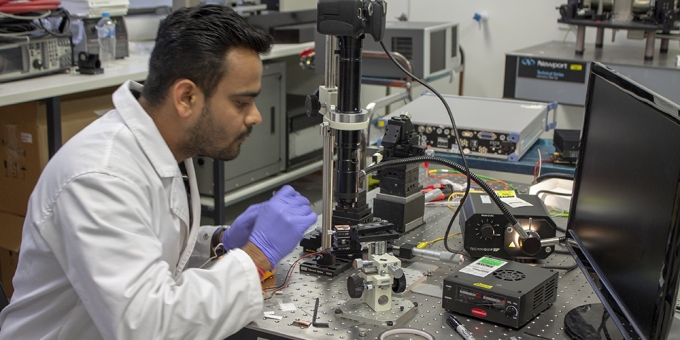
Ankur Sharma, a researcher from The Australian National University, is working on just that. He is creating the next generation of electronic devices, made from organic material.
His research focuses on developing a new class of electronic devices made out of fully recyclable and biodegradable organic semiconductors. Devices made from organic materials would be easy to manufacture, and have a greener environmental footprint.
To realise this, Ankur examines the growth of a novel category of organic semiconductors at the nano scale.
“I focus on a new class of organic two-dimensional (2D) materials that were not grown until recently. These organic materials are of particular interest as they have amazing semiconducting properties. The materials are able to emit light in the visible range, making them suitable for LEDs and other electronics,” Ankur said.
The material Ankur is working with is called ‘pentacene’, and he was able to grow it with one carbon atom thickness. This proved to have excellent semiconducting properties and a visible range band gap, allowing pentacene to be used in LEDs and other light emitting device applications.
“Exfoliation of a single layer of graphene opened up a new class of 2D nanomaterials with interesting semiconducting and insulating properties. But graphene and other similar 2D materials were all inorganic materials. We’ve had the opportunity to study them for the last 5-6 years,” he said.
He is now studying novel 2D organic semiconductors, which are grown only one carbon atom thick. Ankur tested their optoelectronic (processes concerning the combination of electricity and light) and semiconducting properties. At this scale, you can easily manipulate the light-matter interaction to achieve desired properties for electronic devices and Ankur is very pleased with the results.
“We’ve been successful in demonstrating organic materials are suitable semiconductors. They can replace conventional electronic materials like silicon and other plastics and polymers. Plus the performance of these alternative semiconductors is twice as fast as other conventional materials. It paves the way for future optoelectronic devices,” he said.
If these semiconductors are used, Ankur says we can truly realise organic, biodegradable electronic devices. Such a breakthrough would substantially reduce the massive amount of electronic-waste produced around the world.
Until recently, we’ve had limited technology available to recycle all this e-waste. According to Ankur, there are three main challenges to overcome:
- Test the lifecycle durability of the material when higher order currents are being flown through it
- Grow the material on an industrial scale
- Mint the homogeneity and crystallinity for organic materials.
To address the e-waste issue, Ankur aims to propose an alternative material that can be naturally recycled and reduce the amount of waste in landfill.
“The biggest challenge dealing with electronic waste is the energy and the resources required to recycle or dispose of it. That’s why it’s essential that we start looking for alternative semiconductors for all our electronic needs.”
“If we can develop materials that can be recycled naturally with a negative carbon footprint, and still cater to huge electronic market demand-with higher efficiencies; we can resolve the issue of e-waste,” he said.
Ankur hopes his work motivates other material scientists to start working on novel nanomaterials that are environmentally friendly. The potential applications are varied, so in the not-too-distant-future we could see organic and biodegradable solar cells, light emitting diodes, transistors and other electronic devices.
Have a question? Email: ankur.sharma@anu.edu.au